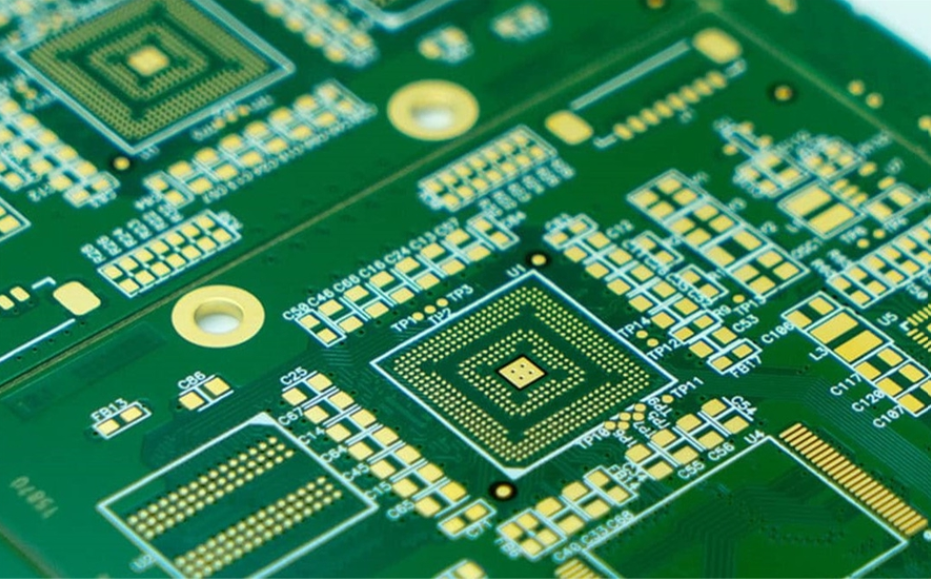
The Shift Toward High-Density Interconnects in Modern Electronics
As modern electronic devices—ranging from advanced medical diagnostics and wearable health monitors to high-speed networking equipment—become increasingly compact, traditional circuit board layouts can no longer support the necessary component density. When engineering teams are forced to route high-pin-count components within a restricted physical footprint, High-Density Interconnect (HDI) technology becomes a mandatory requirement. Transitioning to an HDI architecture allows designers to execute highly complex routing schemes in a fraction of the space. By partnering with a capable Fast Turn PCB provider, hardware teams can leverage these advanced manufacturing techniques to rapidly validate complex, miniaturized designs without sacrificing signal integrity or mechanical reliability.
Core Technologies: Microvias, Fine-Line Routing, and Sequential Build-Up
The foundation of HDI technology is the shift away from standard mechanically drilled through-holes toward precision laser-drilled microvias. These microvias allow for incredibly dense interconnects between adjacent layers, freeing up valuable routing space on the internal planes. This is particularly critical for executing high-density escape routing under tight-pitch BGA (Ball Grid Array) and QFN packages, where standard via geometries simply will not physically fit.
To achieve this extreme density, boards must be manufactured using Sequential Build-Up (SBU) technology. Rather than pressing all layers together in a single lamination cycle, the core is laminated and drilled first, followed by the sequential addition and laser-drilling of outer dielectric layers. A highly capable manufacturing facility must be able to execute various SBU structures with absolute precision, including 1+N+1, 2+N+2, and 3+N+3 architectures. These complex build-ups allow signals to transition across the board with minimal parasitic capacitance, drastically improving high-speed electrical performance.
Impedance Control and Layer Management in High-Density Designs
Packing complex routing into a miniaturized HDI structure introduces severe signal integrity challenges. When traces are routed exceptionally close together using fine-line geometries, cross-talk and impedance mismatches become major risk factors. Therefore, strict layer management and dielectric thickness control are non-negotiable.
The fabrication facility must maintain precise environmental controls during every lamination cycle of a sequential build-up. Any variation in resin flow or laser-drill registration will instantly compromise the localized impedance profile of the high-speed traces. Achieving stable signal performance in these dense layouts requires the manufacturer to maintain strict impedance tolerances and flawless mechanical registration across all sequential layers.
What Buyers Must Verify During Supplier Evaluation
Because HDI fabrication involves multiple high-risk lamination and laser-drilling cycles, it is significantly more complex than standard multi-layer manufacturing. Procurement managers and engineering teams cannot simply assume a supplier is capable based on a marketing brochure. Thoroughly evaluating your HDI PCB manufacturer is a critical procurement step that directly impacts product reliability. Buyers must actively verify the following capabilities before releasing a complex design:
- Sequential Build-Up Expertise: Ensure the facility has verified experience executing up to 3+N+3 HDI structures with reliable microvia plating.
- Trace Geometry Limits: Verify that their fine-line routing capabilities can support your most dense BGA escape patterns.
- Impedance Tolerance: Confirm they can hold strict impedance limits across multiple mixed-dielectric layers.
- Overall Layer Capacity: Ensure their mechanical registration can support high overall layer counts in addition to the HDI microvia structures.
- Pre-Production Engineering Review: Check if their CAM engineers provide deep stack-up analysis to catch structural vulnerabilities before the first lamination cycle.
- Realistic Lead Time: Understand that HDI requires multiple sequential cycles; verify that their quoted schedule is physically realistic for the required build-up.
Advanced Technical Capabilities and Proof Points
To confidently execute complex HDI architectures for critical networking and medical applications, a fabrication facility must possess verified, advanced technical limits. Engineering teams should require the following specific proof points from their manufacturing partner:
- Advanced SBU Structures: Reliable execution of HDI 1+N+1, 2+N+2, and complex 3+N+3 stack-ups.
- Extreme High-Density Routing: Verified 2.5/2.5 mil minimum line/space capabilities for ultra-tight trace routing.
- Massive Layer Capacity: The mechanical alignment and pressing capability to support up to 50 layers.
- Signal Integrity Guarantee: Strict ±5% controlled impedance capability to ensure high-speed transmission lines perform flawlessly.
- Realistic Accelerated Timelines: Delivery of complex HDI builds in around 10 days, depending strictly on the specific sequential design and layer count.
Conclusion
As the demand for smaller, more capable electronic devices continues to grow, HDI technology is transitioning from a specialized niche to an industry standard. However, the multi-cycle complexity of HDI fabrication leaves zero room for manufacturing errors. By thoroughly evaluating suppliers on their technical execution of microvias, sequential build-ups, and precise impedance control, engineering and procurement teams can eliminate the risk of latent field failures. Partnering with a facility that offers robust pre-production engineering support and verified technical capabilities ensures that your most advanced high-density designs are brought to market successfully, reliably, and on schedule.